X-ray photoelectron spectroscopy (XPS)
As the demand for high performance materials increases, so does the importance of surface engineering. The material’s surface is the point of interaction with the external environment and other materials, therefore many of the problems associated with modern materials can be solved only by understanding the physical and chemical interactions that occur at the surface, or at the interfaces of a material’s layers. The surface will influence such factors as corrosion rates, catalytic activity, adhesive properties, wettability, contact potential and failure mechanisms.
Surface modification can be used to alter or improve these characteristics, and so surface analysis is used to understand surface chemistry of a material, and investigate the efficacy of surface engineering. From non-stick cookware coatings to thin-film electronics and bio-active surfaces, X-ray photoelectron spectroscopy is one of the standard tools for surface characterization.
X-ray photoelectron spectroscopy (XPS), also known as electron spectroscopy for chemical analysis (ESCA), is a technique for analyzing the surface chemistry of a material. XPS can measure the elemental composition, empirical formula, chemical state and electronic state of the elements within a material. XPS spectra are obtained by irradiating a solid surface with a beam of X-rays while simultaneously measuring the kinetic energy and electrons that are emitted from the top 1-10 nm of the material being analyzed. A photoelectron spectrum is recorded by counting ejected electrons over a range of electron kinetic energies. Peaks appear in the spectrum from atoms emitting electrons of a particular characteristic energy. The energies and intensities of the photoelectron peaks enable identification and quantification of all surface elements (except hydrogen).
Surface Characterization
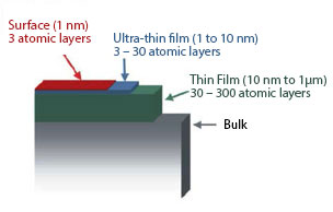
A surface layer is defined as being up to three atomic layers thick (~1 nm), depending upon the material. Layers up to approximately 10 nm are considered ultra-thin films, and layers up to approximately 1 μm are thin films. The remainder of the solid is referred to as bulk material. This terminology is not definitive however, and the distinction between the layer types can vary depending upon the material and its application.
The surface represents a discontinuity between one phase and another and, therefore, the physical and chemical properties of the surface are different from those of the bulk material. These differences affect the topmost atomic layer of the material to a large extent. In the bulk of the material, an atom is surrounded on all sides in a regular manner by atoms composing that material. Because a surface atom is not surrounded by atoms on all sides, it has bonding potential, which makes the surface atom more reactive than atoms in the bulk.
Surface Properties
Common properties and processes as a function of the depth or thickness that is important for the specific properties or processes. Surface analysis contributes to the understanding for each of these areas
- Semiconductor/ Microelectronics
- Microcircuits
- Ultra-thin Films
- Soldering
- Cleaning
- Thin-film Stability
- Barrier Layers
- Lubrication
- Chemical Industry
- Plastics/Coatings
- Catalysis
- Fibers
- Metal/Steel Industry
- Nitriding/Carburizing
- Corrosion
- Welding
- Fatigue
- Grain boundary segregation
- Glass
- Coatings
- Motor/Avionics
- Lubrication
- Corrosion
- Oxidation
- Fatigue/Failure
- Fiber Composites
- Adhesives
Some of the areas of technology in which surfaces and surface analysis are important include the following:
The Photoemission Process
When an atom or molecule absorbs an X-ray photon, an electron can be ejected. The kinetic energy (KE) of the electron depends upon the photon energy (hν) and the binding energy (BE) of the electron (i.e., the energy required to remove the electron from the surface).
The photoemission process involved for XPS surface analysis. The discs represent electrons and the bars represent energy levels within the material being analyzed. The equation governing the process is: KE = hν - BE
By measuring the kinetic energy of the emitted electrons, it is possible to determine which elements are near a material’s surface, their chemical states and the binding energy of the electron. The binding energy depends upon a number of factors, including the following:
- The element from which the electron is emitted.
- The orbital from which the electron is ejected
- The chemical environment of the atom from which the electron was emitted.
XPS is a quantitative technique because the cross-section for the emission of a photoelectron is not dependent upon the chemical environment of the atom.